
Enhancing Sputtering Magnetron Design
Improved Deposition Rate, Target Utilization, and Uniformity
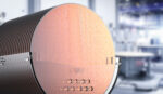
Sputtering magnetrons are indispensable components in various industries, including, semiconductor, hard disk drive, optical coatings, and implantable medical devices. The optimization of these magnetrons is pivotal for achieving superior performance in deposition rates, maximizing target utilization, and ensuring film uniformity. In this exploration, we delve into the essential factors that contribute to enhancing sputtering magnetron design for unparalleled results across diverse applications.
Deposition Rate Optimization
Increasing Power: Enhancing cooling efficiency and thermal conductivity facilitates the operation of sputtering at peak power levels. Utilizing bolt-on or bonded target configurations, along with conductive pastes or epoxies, improves thermal conductivity, ensuring maximum power density specific to the target material.
Decreasing Source-Substrate Distance: The proximity between the target and substrate directly impacts sputtering rates. Maintaining a shorter source-substrate distance optimizes sputtering efficiency, albeit with diminishing returns beyond an optimal range.
Lowering Operating Pressures: Regulating gas flow in the chamber minimizes atom and ion collisions, thereby augmenting material ejection rates from the target surface. Lower operating pressures translate to higher achievable sputtering rates.
Maximizing Target Utilization:
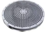
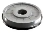
- Optimize Magnetic Field: Magnetron design plays a pivotal role in target utilization. By optimizing the magnetic field, magnetron efficiency can be significantly enhanced, with potential target utilization improvements from 20–30% to 50–60%. Techniques such as omitting the central part of the target or implementing motion in the magnetic circuit can achieve full target erosion.
- Scanning Magnetic Field: Introducing motion to the magnetic circuit beneath the target surface expands the area exposed to the sputtering discharge, ensuring uniform erosion across the target surface.
Achieving uniformity in sputtering applications requires a multifaceted approach:
Enhancing uniformity involves collaboration between magnetron suppliers and process development engineers to optimize performance and reduce ownership costs.
Practical Tips and Advice:
- Collaborate with Magnetron Suppliers: Engage closely with magnetron suppliers to optimize magnetron design for specific applications, ensuring compatibility with system requirements and process goals.
- Systematic Testing and Optimization: Conduct thorough testing and optimization of magnetron parameters within the sputtering system to fine-tune performance and achieve desired outcomes.
- Continuous Monitoring and Maintenance: In addition, implement routine monitoring and maintenance protocols to uphold magnetron performance and prolong operational lifespan, safeguarding consistent deposition quality.
Example Applications:
- Semiconductor Thin Films: Precise control over deposition rate and uniformity is essential for semiconductor fabrication, ensuring the integrity and functionality of thin film components.
- Optical Coatings: Uniform film thickness and high deposition rates are critical for optical coatings to maintain optical clarity and performance.
- Medical Device Coatings: Uniform and adherent coatings on medical devices are imperative for biocompatibility, corrosion resistance, and functional performance.
- Photovoltaics: Consistent film uniformity and optimized deposition rates are vital for enhancing the efficiency and longevity of photovoltaic cells.
- Large Area Glass: Uniform coatings on large area glass substrates are essential for optical clarity, durability, and aesthetic appeal.
- Packaging Coatings: Deposition rate optimization and uniformity ensure the integrity and functionality of packaging coatings, enhancing product shelf life and performance.
In conclusion, optimizing sputtering magnetron design is paramount for achieving enhanced deposition rates, maximizing target utilization, and ensuring film uniformity across diverse applications. By leveraging innovative design strategies and collaborative partnerships, engineers can unlock the full potential of sputtering technology. As a result, this drives advancements in industries ranging from semiconductor manufacturing to medical device development. Schedule a meeting to learn how Dexter can help you optimize magnetron performance.
References:
- P. K. Tushinskiy et al., “Design and optimization of magnetron sputtering systems for deposition of high-quality thin films,” *Journal of Physics: Conference Series,* vol. 574, no. 1, p. 012040, 2015.
- C. Mitterer et al., “Magnetron sputtering—The power of modern technology for thin film deposition,” *Materials Science and Engineering: A,* vol. 342, no. 1-2, pp. 159-167, 2003.
- D. M. Mattox, *Handbook of Physical Vapor Deposition (PVD) Processing,* 2nd ed. Norwich, NY: Elsevier Science, 2010.