
The Physics and Theory of Sputtering
Sputtering is a physical vapor deposition (PVD) process used to deposit thin films of material onto a substrate. The process involves bombarding target material with energetic particles, typically ions of an inert gas like argon, which causes ejection of atoms from the target. These atoms land on the substrate and create the film.
Discovery:
Sputtering was first observed by William Robert Grove in 1852 during his experiments with glow discharge tubes. However, it wasn’t until the 1940s and 1950s that sputtering began to be developed as a practical thin film deposition technique.
Required conditions/system:
- High vacuum chamber (typically 10^-5 to 10^-7 Torr before gas introduction)
- Inert gas supply (usually argon)
- Power supply (DC, RF, or pulsed DC)
- Cooling system for the target
- Substrate holder (often with heating/cooling capabilities)
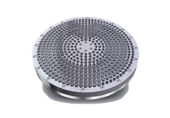
- Magnetron assembly (for magnetron sputtering)
Magnetron Sputtering
Magnetron sputtering is an enhanced form of sputtering that uses strong magnetic fields to trap electrons near the target surface. This increases the probability of electron-atom collisions, which leads to higher ionization rates and, consequently, higher sputtering rates.
How magnetrons work:
- Magnets are placed behind the target material.
- The magnetic field lines run parallel to the target surface and perpendicular to the electric field.
- Electrons are trapped in this magnetic field, following helical paths around the magnetic field lines.
- This increases the electron density near the target, leading to more ionization events and a denser plasma.
- The result is a higher sputtering rate and more efficient use of the target material.
Role of magnetics:
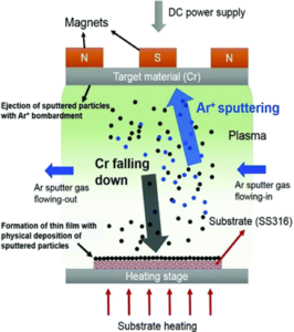
The magnetic field is crucial in confining the plasma close to the target surface. This confinement increases the sputtering efficiency and allows operation at lower pressures, which can lead to higher quality films.
Types of magnets used:
- Permanent magnets: Most common, especially in smaller systems. They provide a constant magnetic field without requiring power.
- Electromagnets: Allow for adjustable magnetic fields, which can be beneficial for process control. They require power and cooling.
- Hybrid magnets: Combine permanent magnets with electromagnets, offering a balance between field strength and adjustability.
Materials
- Metals (e.g., aluminum, copper, gold, titanium)
- Alloys (e.g., stainless steel, nichrome)
- Semiconductors (e.g., silicon, germanium)
- Insulators (e.g., silicon dioxide, aluminum oxide)
- Ceramics (e.g., titanium nitride, zirconium oxide)
Substrates:
- Silicon wafers
- Glass
- Polymers (e.g., polyethylene terephthalate, polyimide)
- Metals (e.g., steel, aluminum)
- Ceramics
- Organic materials (in some specialized applications)
Sputtering Technologies
Different sputtering technologies are suited to various target and substrate combinations:
DC Magnetron Sputtering:
- Used for conductive materials (metals and alloys)
- High deposition rates
- Simple and cost-effective
Pulsed Magnetron Sputtering:
- Useful for reactive sputtering of dielectric materials
- Helps prevent arcing and target poisoning
- Allows better control of film properties
RF Sputtering:
- Used for non-conductive materials (insulators and semiconductors)
- Prevents charge buildup on the target
- Generally slower deposition rates than DC
Reactive Sputtering:
- Introduces a reactive gas (e.g., oxygen or nitrogen) to form compound films
- Used for oxides, nitrides, and carbides
- Requires careful process control to maintain stoichiometry
Co-sputtering:
- Uses multiple targets to deposit alloys or doped materials
- Allows fine control of composition
- Useful for research and development of new materials
HIPIMS (High Power Impulse Magnetron Sputtering):
- Uses very high-power pulses with low duty cycles
- Produces highly ionized plasma and energetic sputtered atoms
- Results in denser films with improved adhesion
- Useful for hard coatings and filling high aspect ratio features
Critical Aspects of Magnetron Design
Key considerations in magnetron design include:
- Magnetic field strength and configuration
- Target cooling efficiency
- Erosion profile and target utilization
- Power delivery and impedance matching
- Ease of maintenance and target replacement
- Scalability for larger area coatings
Principal Applications and Industries
- Integrated circuit metallization
- Magnetic storage media
- Systems: Cluster tools, in-line systems
Optics and Displays:
- Anti-reflective coatings
- Transparent conductive oxides (e.g., ITO)
- Systems: Large area coaters, roll-to-roll systems
Automotive:
- Decorative coatings
- Hard, wear-resistant coatings
- Systems: Batch coaters, carousel systems
- Thermal barrier coatings
- Corrosion-resistant coatings
- Systems: Large batch coaters
Solar Industry:
- Thin-film solar cells
- Anti-reflective coatings
- Systems: Inline systems, roll-to-roll coaters
- Biocompatible coatings
- Antimicrobial surfaces
- Systems: Small batch coaters
Emerging Technologies
- Flexible electronics: Deposition on polymer substrates
- OLED displays: Thin-film encapsulation layers
- Quantum computing: Superconducting thin films
- Neuromorphic computing: Memristive materials
- Energy storage: Thin-film batteries and supercapacitors
- Photonics: Metamaterials and photonic crystals
- Wearable technology: Conductive and protective coatings
At Dexter, we specialize in developing and manufacturing cutting-edge magnetron sputtering systems. Our team of experts can support you in:
- Designing custom magnetrons tailored to your specific application
- Optimizing your sputtering processes for maximum efficiency and quality
- Scaling up your production with our advanced large-area coating solutions
- Providing ongoing technical support and maintenance services
Whether you’re in R&D or high-volume production, our magnetron technology can help you achieve your thin film deposition goals. Contact us today to discuss how we can enhance your sputtering capabilities and drive innovation in your industry.